CEA-Leti Scales FeRAM Memory to 22nm for Edge AI
French research institute CEA-Leti has demonstrated ferroelectric RAM scaled to 22nm using a novel 3D capacitor design for edge AI.
What Happened
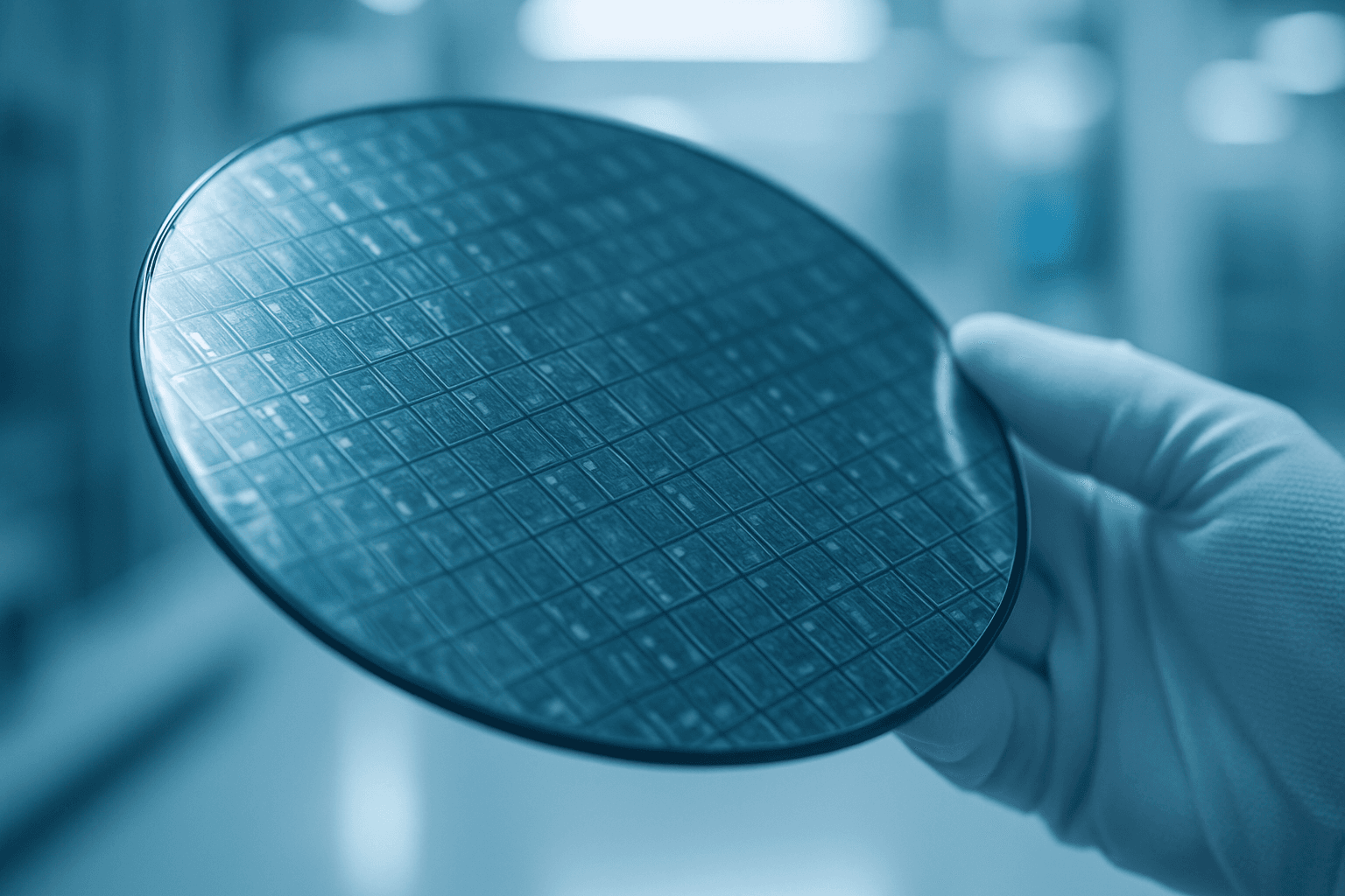
French semiconductor research institute CEA-Leti has demonstrated ferroelectric random-access memory, known as FeRAM, scaled to the 22nm manufacturing node, using a novel three-dimensional capacitor architecture. The announcement marks a significant step in bringing non-volatile memory technology to the process nodes required for modern edge AI hardware.
Background
FeRAM is a type of non-volatile memory that stores data using ferroelectric materials rather than the charge-based mechanisms used in conventional flash memory. The technology offers lower power consumption and faster write speeds compared to flash, characteristics that have made it a subject of interest for embedded and edge computing applications, where energy efficiency and responsiveness are constrained by battery capacity and real-time processing requirements.
CEA-Leti, the microelectronics and nanotechnology laboratory of the French Alternative Energies and Atomic Energy Commission, is based in Grenoble, France. The institute operates as a research and technology organisation focused on bridging fundamental science and industrial application, with a particular concentration on semiconductor process development. CEA-Leti has existing partnerships with major semiconductor manufacturers and has previously contributed to advances in silicon photonics, MEMS, and advanced packaging technologies.
Scaling FeRAM to smaller process nodes has historically presented manufacturing challenges. Ferroelectric capacitors require specific material properties that can degrade or become difficult to control as dimensions shrink. Prior commercial FeRAM deployments have generally remained at larger nodes, limiting integration density and constraining the technology's competitiveness against alternative non-volatile memory types such as MRAM and ReRAM at advanced nodes.
The Technical Approach
CEA-Leti's demonstration addresses the scaling challenge through a three-dimensional capacitor design. By building the capacitor structure vertically rather than in a planar configuration, the design allows the ferroelectric material to retain sufficient volume and surface area to maintain reliable switching behaviour at the 22nm node. The institute has not disclosed the specific ferroelectric material used in this iteration, though hafnium oxide-based ferroelectrics have been the dominant focus of the research community for CMOS-compatible FeRAM development in recent years.
The 22nm node is significant because it aligns with process generations used in a broad range of embedded microcontrollers, application processors, and dedicated AI inference chips deployed at the edge, including in industrial sensors, automotive systems, and IoT devices.
Relevance to Edge AI
Edge AI applications require hardware that can perform inference tasks locally, without continuous connectivity to cloud infrastructure. This places demands on memory systems to store model weights and intermediate data with minimal energy draw and latency. Non-volatile memory integrated directly with processing logic reduces the need to transfer data across separate chips, a process that consumes both power and time.
FeRAM's combination of non-volatility, low write energy, and byte-addressability, meaning individual memory locations can be written without erasing entire blocks, makes it a candidate for storing model parameters in power-constrained edge deployments. Scaling the technology to 22nm increases the amount of memory that can be embedded within a given chip area at that process node.
CEA-Leti described the demonstration as targeting edge AI applications, though the institute has not announced a specific commercial partner or production timeline in the current wire reports.
Industry Context
The push to advance non-volatile memory at competitive process nodes reflects broader demand from the semiconductor industry for memory solutions that can keep pace with AI workload requirements at the edge. Established memory makers and research institutions have pursued multiple competing technologies in parallel, and no single approach has achieved dominant commercial adoption at advanced nodes for embedded AI use cases.
CEA-Leti is expected to present further technical details of the 22nm FeRAM demonstration through forthcoming research publications and industry conference proceedings.
Get our editors' take on what it all means. Read the Editor's Blog →