Huawei Claims New Chip Architecture Can Match 1.4nm by 2031
Huawei announced a new semiconductor design architecture it says will produce 1.4nm-class chips by 2031 without EUV lithography.
Huawei Claims New Chip Architecture Can Match 1.4nm by 2031
Huawei Technologies announced Monday a new semiconductor design methodology it says will enable the company to produce chips equivalent to the 1.4-nanometer class by 2031, without relying on extreme ultraviolet lithography equipment that the United States has blocked China from obtaining. The announcement, made at a company event, represents Huawei's most detailed public claim yet about its path to advanced chip manufacturing under continued U.S. export restrictions.
What Was Announced
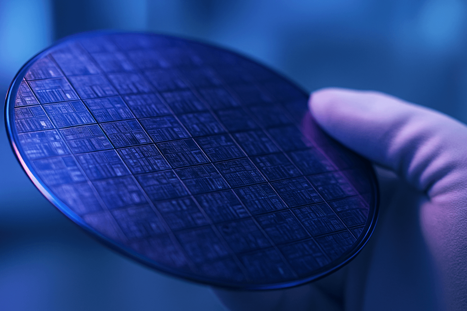
Huawei said its new approach, called LogicFolding, is a chip architecture that the company claims achieves 55 percent higher transistor density compared to conventional planar designs. The company said LogicFolding restructures how transistors are arranged on a die, allowing more computing elements to be packed into the same physical space without requiring the sub-angstrom-wavelength lithography tools that leading-edge fabrication currently depends on.
Alongside the architecture announcement, Huawei introduced what it is calling the Tau Scaling Law, a framework the company says it intends as a successor to Moore's Law. Moore's Law, the observation that transistor counts on chips double roughly every two years, has guided semiconductor development targets for decades. Huawei did not provide detailed technical specifications of the Tau Scaling Law in publicly available materials reviewed by wire services.
Huawei said its flagship Mate 90 series of consumer processors will be the first commercial products to incorporate the LogicFolding architecture.
Background
Huawei has operated under sweeping U.S. export restrictions since 2019, when the Department of Commerce placed the company on its Entity List, cutting off access to American-designed components and software. Subsequent rules have extended those restrictions to foreign companies using U.S. technology in their supply chains, effectively limiting Huawei's access to chips manufactured by leading foundries including Taiwan Semiconductor Manufacturing Company.
In 2023, Huawei drew international attention when its Mate 60 Pro smartphone was found to contain a 7nm chip produced by Semiconductor Manufacturing International Corporation, China's largest domestic chipmaker. SMIC is also subject to U.S. export controls that restrict its access to advanced manufacturing equipment. Analysts at the time noted that SMIC appeared to have produced the 7nm chip using older deep ultraviolet lithography tools rather than EUV equipment.
EUV lithography machines, produced almost exclusively by the Dutch company ASML, are considered essential for manufacturing chips at 5nm and below using conventional methods. The Dutch government, under pressure from Washington, has restricted ASML from shipping its most advanced EUV systems to China.
What the Claims Involve
Huawei's announcement centers on the assertion that the LogicFolding architecture can compensate for the absence of EUV lithography by changing how chip structures are designed rather than how they are printed. The company said this approach would allow it to reach performance levels comparable to chips produced at 1.4nm using available manufacturing processes.
Reuters reported that Huawei said it expects to be making industry-leading semiconductors using the new technology within five years, which would place that target around 2031. The company did not name a manufacturing partner or specify which foundry would produce chips using the LogicFolding method.
Independent verification of Huawei's technical claims was not available at the time of publication. The company has not submitted the LogicFolding architecture or the Tau Scaling Law for external peer review, according to available reports.
Industry Context
The 1.4nm process node is currently in development at TSMC and Samsung. TSMC has indicated it expects to begin risk production of its N2 node, roughly equivalent to 2nm, in 2025, with further shrinks to follow. Intel has its own 14A node, which it describes as 1.4nm-class, targeted for the latter half of the decade.
If Huawei's claims are borne out, Chinese domestic chip production could narrow a gap that U.S. policymakers have sought to maintain through successive rounds of export controls.
Huawei said the Mate 90 series will serve as the first commercial demonstration of the LogicFolding architecture, though the company has not announced a release date for that product line.
Get our editors' take on what it all means. Read the Editor's Blog →