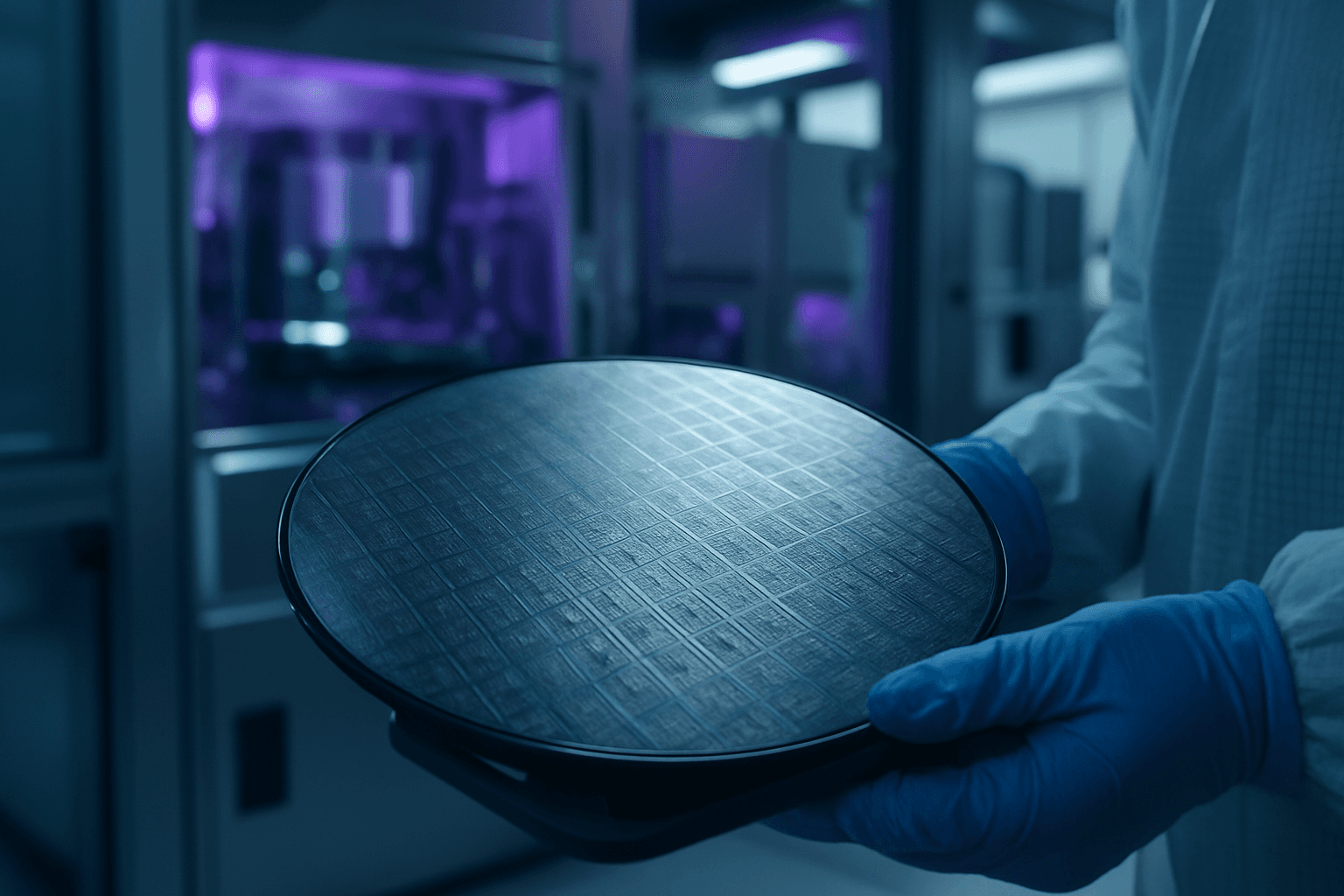
Imec Fabricates First Quantum Dot Qubit Using High-NA EUV
Imec has built the world's first quantum dot qubit device fabricated using High-NA EUV lithography, the same tooling used for next-generation AI chips.
Imec Fabricates First Quantum Dot Qubit Device Using High-NA EUV Lithography
Belgian semiconductor research consortium Imec announced it has fabricated the world's first quantum dot qubit device using High-NA extreme ultraviolet (EUV) lithography, the same advanced manufacturing technology being adopted for the most advanced conventional AI and logic chips. The development places quantum computing device fabrication on the same industrial manufacturing roadmap used by leading commercial chipmakers for the first time.
What Happened
Imec confirmed the fabrication of a quantum dot qubit device using High-NA EUV lithography equipment. High-NA EUV is the latest generation of extreme ultraviolet lithography, offering higher numerical aperture optics that enable finer patterning resolution than the previous EUV generation. Until this announcement, quantum dot qubit devices had not been produced using this class of tooling.
The qubit devices are based on quantum dots, small semiconductor structures that can confine individual electrons and serve as the physical basis for quantum bits. Fabricating these structures with High-NA EUV allows feature sizes and patterning precision comparable to those used in leading-edge conventional semiconductor manufacturing.
Background
Imec, headquartered in Leuven, Belgium, operates as an independent research and development organization working with chipmakers, equipment suppliers, and materials companies across the global semiconductor industry. Its fabrication facilities are used to prototype and validate manufacturing processes that are later adopted at commercial scale by industry partners including TSMC, Samsung, and Intel Foundry.
High-NA EUV tools are currently being deployed by TSMC and Intel for sub-2nm logic chip production. ASML, the sole supplier of EUV lithography systems globally, began delivering High-NA EUV systems to leading chipmakers in 2024. The tools cost approximately 380 million euros each and are considered critical infrastructure for the most advanced nodes in conventional semiconductor manufacturing.
Quantum computing hardware has historically been fabricated using older lithography generations or highly customized processes not compatible with mainstream semiconductor manufacturing lines. This has been cited as a barrier to scaling quantum hardware to the volumes and densities required for commercially relevant systems.
What Was Demonstrated
By using High-NA EUV to fabricate a functional quantum dot qubit device, Imec demonstrated that quantum hardware can, in principle, be produced on the same equipment and within the same fab environments being prepared for next-generation conventional chips. The fabrication process used standard semiconductor manufacturing flows rather than bespoke quantum-specific processes.
Imec did not announce qubit performance specifications, coherence times, or error rates in connection with this fabrication milestone. The announcement focused on the manufacturing method and its compatibility with mainstream chipmaking infrastructure rather than on qubit operational metrics.
What It Means in Practice
The significance of the result lies in manufacturing compatibility rather than raw qubit performance. If quantum dot qubit devices can be fabricated using the same tools and process flows as conventional chips, it opens the possibility of producing quantum hardware at the same facilities, and eventually at similar volumes and cost structures, as standard logic devices.
This manufacturing alignment could reduce one of the principal bottlenecks in quantum hardware scaling: the need for separate, specialized fabrication infrastructure. Existing High-NA EUV capacity being built out by chipmakers for AI accelerator and logic chip production could, under this approach, be applied to quantum device manufacturing without requiring entirely separate fab lines.
Imec has not announced a timeline for transitioning this fabrication approach from research demonstration to production-scale use, nor have commercial chipmaker partners confirmed plans to adopt the process for quantum hardware manufacturing.
Imec is expected to present further technical details of the fabrication process and device characteristics at upcoming semiconductor research conferences, where peer scrutiny of the methodology and device data will follow.
Get our editors' take on what it all means. Read the Editor's Blog →